

 ENGLISH
R&D Design Area
-
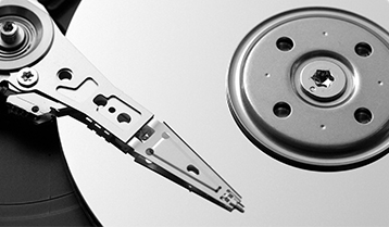 Semiconductor equipment precision parts designing
We research and develop semiconductor cleaning equipment parts utilized in precision cleaning equipment of 300mm Silicon Wafer.
-
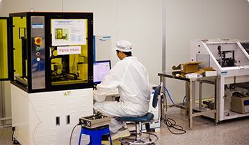 Micro Droplet Technology
We are the only company in the world that developed the technology to control the diameter and velocity of liquid droplet within 2% standard deviation.
-
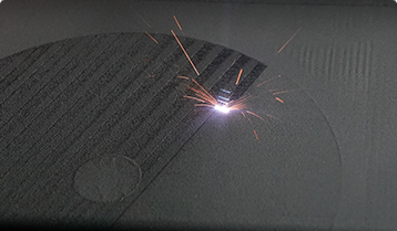 parts elementary technology
The Company researches and develops parts elementary technology that combines parts elementary technology precision processing and 3D printing process.
R&D Design Achievement.
-
- 2017
-
Developed nozzles for top global equipment company.
Conducted the national project, 「Development of LED Heater-based Wafer heating Chuck」
-
- 2016
-
Supplied Wafer Cleaning TEST equipment to Seoul National University; HPU for Nozzle-based Wafer Cleaning TEST.
Developed Flow Cell using the Company’s own processing technology.
Developed HS Twin Fluid Nozzle for semiconductor cleaning.
Supplied KYUNG HEE UNIVERSITY laboratory equipment HPU for bead generation experiment.
-
- 2015
-
Developed Polymer and Quartz Slit Nozzle for S Company.
-
- 2013
-
Begun the development of Wafer Heating Chuck: Chuck with heat source capable of heating the lower part of Wafer.
-
- 2012
-
Conducted the national project,
「Development of Micro Droplet Nozzle capable of cleaning micropattern (jointly with Company S)」